Merancang dan Membuat Single/Double Layer PCB Secara Manual dengan Metode Eksposure: DIY Guide! Cara membuat pcb dengan metode manual cuter – blogkamarku
So, you got your electronics, right? And inside them, there's this green (or sometimes other colors) board covered in lines and little components. That's the PCB, baby. It's what connects all the transistors, resistors, and chips together and lets them do their thing. We gonna talk about single layer PCBs, cause you gotta start somewhere, right?
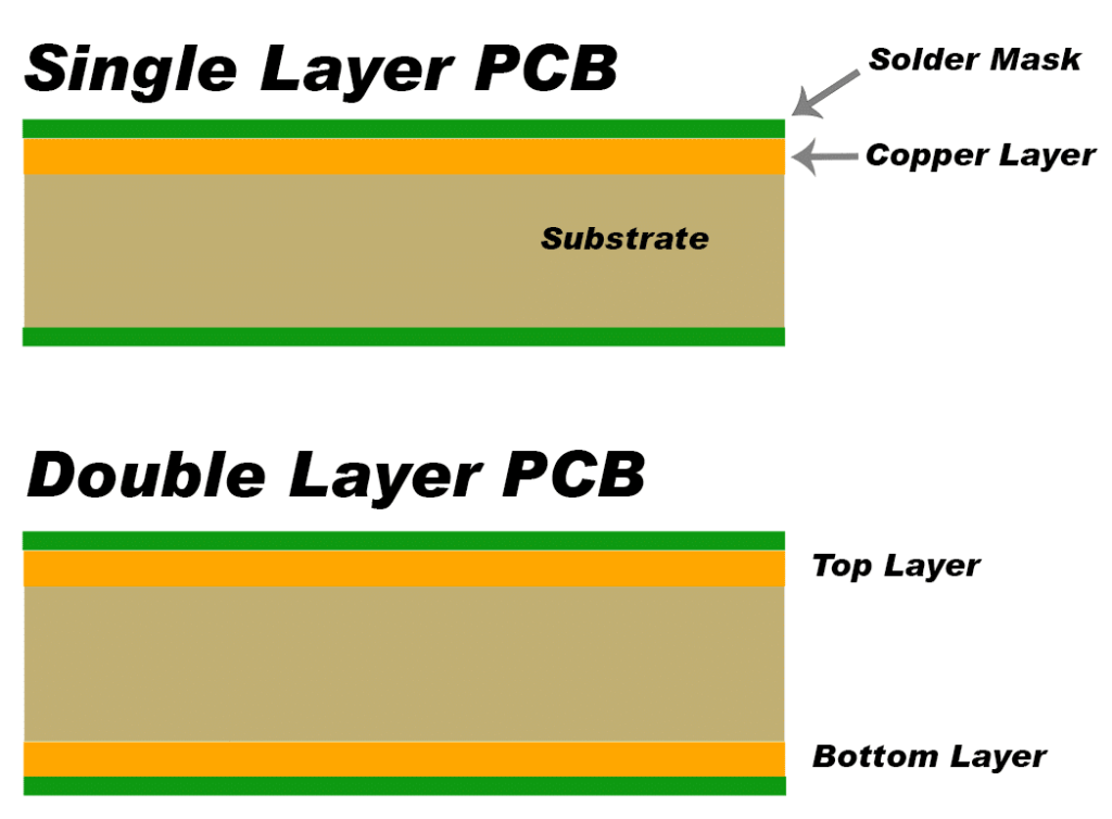
Understanding Single Layer PCBs

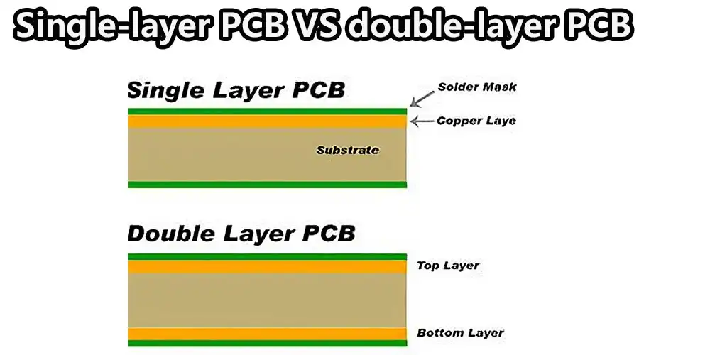
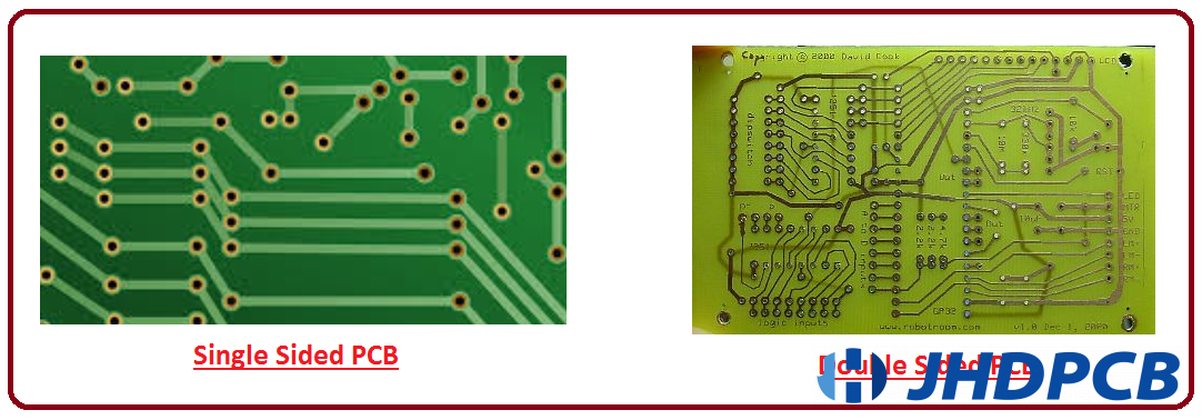
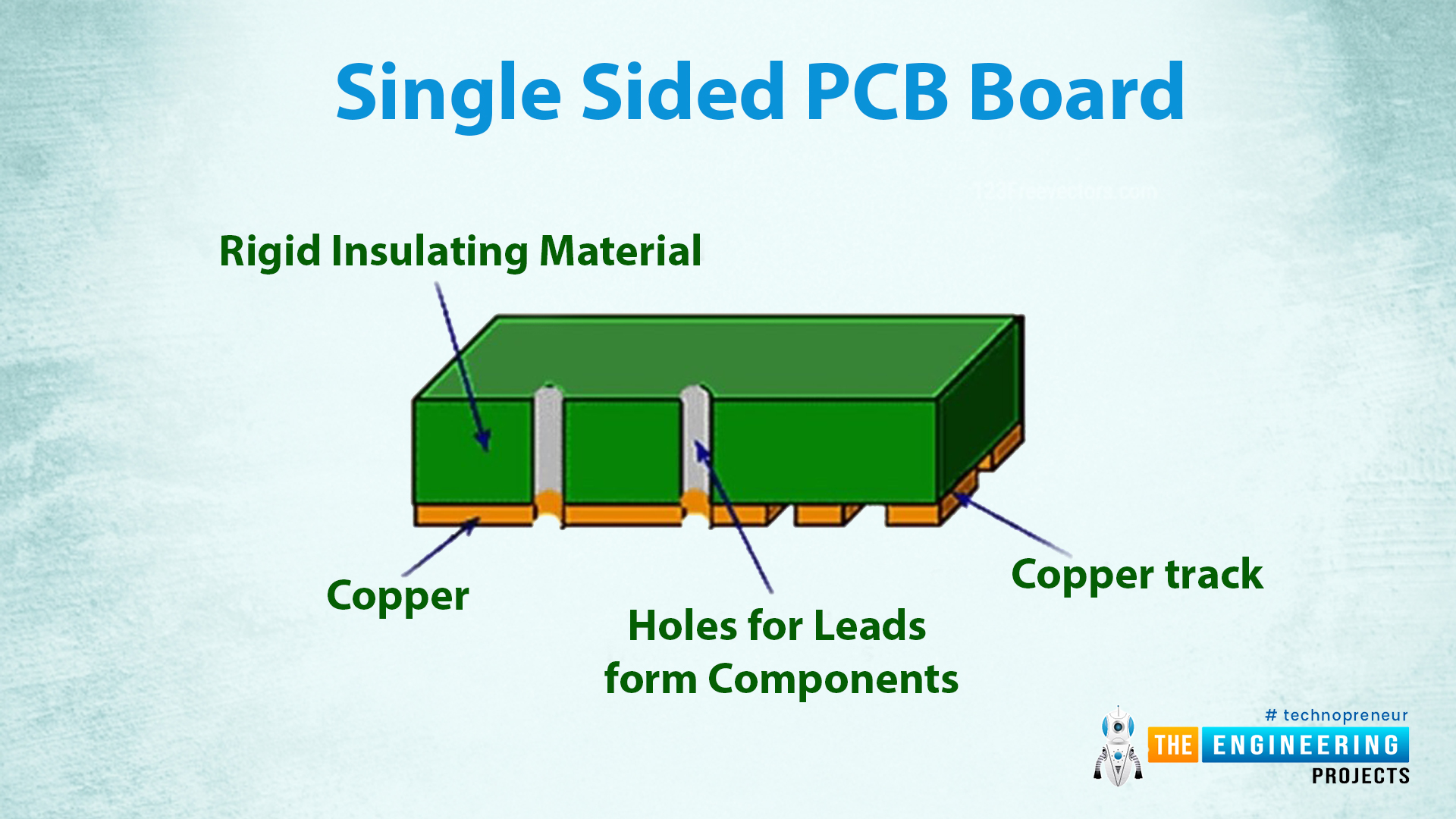
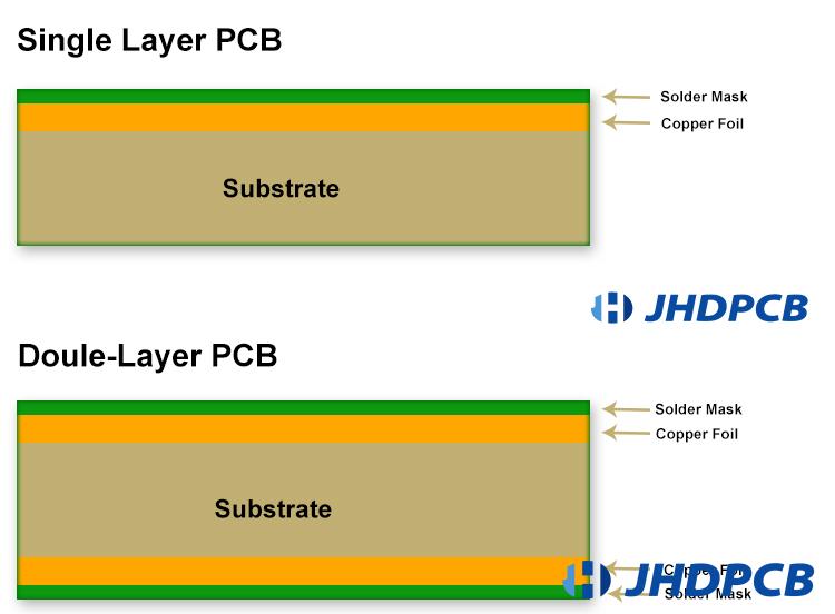
Now, a single layer PCB is the simplest form. Imagine a slice of bread, but instead of peanut butter, you got a thin layer of copper on one side. That copper is etched away, leaving behind the conductive pathways – the "traces" – that connect all the components. These PCBs are used in simpler devices. Think about your old calculator, or maybe that remote control that you had back in the days. Simple stuff. Cheaper to manufacture and easier to design. They're like the basic building blocks of the electronic world. But here's the thing: they can get messy quick! With only one layer to work with, routing those traces can become a real headache. You gotta be clever with your layout, find ways to weave those lines around, or use jumper wires to hop over each other. Think of it like trying to untangle a bunch of Christmas lights, but on a tiny scale.
Delving into Single & Double Layer PCB
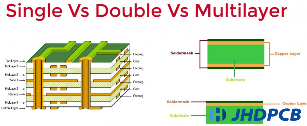
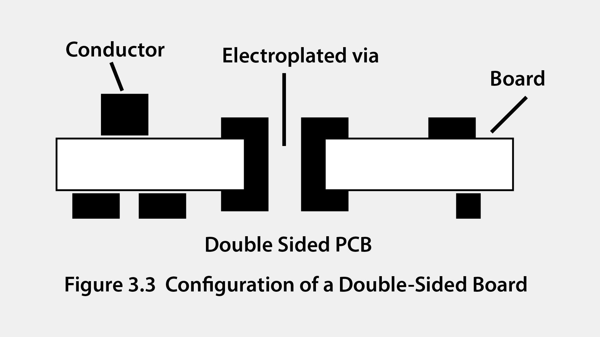
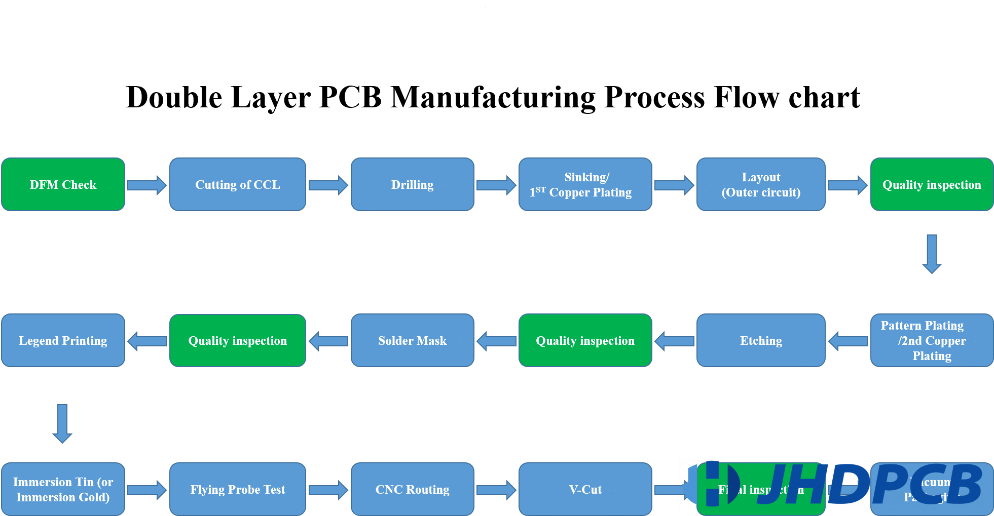
Now, after you master your single layer, you move on to double layer. These boards got copper on both sides, giving you twice the real estate for your traces. This means you can pack more components onto a smaller board, and the routing becomes way easier. It's like going from a one-lane road to a two-lane highway. More space, less congestion. Double-sided PCBs are in everything from computers to home appliances. It's a step up in complexity and cost. Think about it: you can have components on both sides of the board, and you can connect them through "vias" – little holes that are plated with copper, that allows a signal to travel from one side to the other. These vias are what allows you to build a complex circuit on a double-layer board. Choosing between single and double layer is a matter of balancing complexity, cost, and space. For simple circuits, a single-layer board is perfectly fine. But when you need more features, more components, or just a smaller footprint, a double-layer board is the way to go. Don't you go putting a double layer when a single can do. So next time you crack open an old gadget, take a peek at the PCB inside. You might just be surprised at how much technology is packed into that little green board. From simple calculators to advanced computers, PCBs are the unsung heroes of the electronic world. Keep learning, stay curious, and always respect the tech, homie!
If you are searching about Introduction to Double Layer PCB - The Engineering Projects you've came to the right page. We have 25 Images about Introduction to Double Layer PCB - The Engineering Projects like Double Layer PCB | Construction And Applications, Single & Double Layer PCB - Jhdpcb and also Introduction to Double Layer PCB - The Engineering Projects. Here it is:
Introduction To Double Layer PCB - The Engineering Projects
 pcb-design.pages.dev
 What Is Double-layer PCB And How Is It Made - Complete Guide - IBE
 www.pcbaaa.com
 Understanding Double Layer PCB - PCBA Manufacturers
 www.pcba-manufacturers.com
 Meng-Assembly Komponen Elektronika Pada PCB Secara Manual – Teknik
 skansatv.smkn1bawang.sch.id
 Membuat Pola Sesuai Style Dan Spesifikasi Secara Manual – Tata Busana
 skansatv.smkn1bawang.sch.id
 Single & Double Layer PCB - Jhdpcb
 www.jhdpcb.com
 MEMBUAT JALUR DI PCB SECARA MANUAL | SUTONOENZU
 sutonoenzu.blogspot.com
 pcb jalur membuat cara elektronik komponen lukisan boards praktis secara bahan jenis2 rangkaian untuk elektronika paling saya hai merupakan membahas
What Is The Better PCB: 2 Layer Vs 4 Layer PCB?
 www.pcbmay.com
 What Is Double-layer PCB And How Is It Made - Complete Guide - IBE
 www.pcbaaa.com
 Single & Double Layer PCB - Jhdpcb
 www.jhdpcb.com
 What Is Double-layer PCB And How Is It Made – Complete Guide |Qtech
 qtech-us.com
 Cara Membuat PCB Dengan Metode Manual Cuter – BLOGKAMARKU
 blogkamarku.blogspot.com
 Tips Praktis Perakitan PCB (Printed Circuit Board) Secara Manual
 secara manual.webp) elektronikamag.tistory.com
elektronikamag.tistory.com Single & Double Layer PCB - Jhdpcb
pcb-design.pages.dev MERANCANG DAN MEMBUAT SINGLE LAYER PCB – Bian Hardiyanto, S.T
catatanharianinstruktur.wordpress.com pcb merancang layer circuit kesimpulan
What Is Double-layer PCB And How Is It Made - Complete Guide - IBE
 www.pcbaaa.com
 Single & Double Layer PCB - Jhdpcb
 pcb-design.pages.dev
 Introduction To Single Layer PCB - The Engineering Projects
 pcb-design.pages.dev
 Double Layer PCB | Construction And Applications
 pcb-design.pages.dev
 Single & Double Layer PCB - Jhdpcb
 pcb-design.pages.dev
 How To Choose The Most Suitable Layer Number For PCB Design – PCB HERO
 www.pcb-hero.com
 Merancang Dan Membuat Single/ Double Layer PCB Secara Manual Dengan
 skansatv.smkn1bawang.sch.id
 √ Merancang Dan Membuat Single /Double Layer PCB (Printed Circuit Board
 www.mekaelektronika.com
 Cara Membuat PCB Dengan Metode Manual Cuter – BLOGKAMARKU
 blogkamarku.blogspot.com
 membuat pcb metode cuter
Melakukan Pemeriksaan PCB Assembly Secara Visual/Manual – Teknik
 skansatv.smkn1bawang.sch.id
 What is double-layer pcb and how is it made. What is double-layer pcb and how is it made. Merancang dan membuat single/ double layer pcb secara manual dengan